The MIPS Register File
- We observed from figure 4.15 page 263, the register file has the followin configuration
-
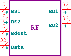
- Notice they prvide slightly different labels in their diagrams,
- RS1 is Read Register 1, RS2 is Read Register 2, ...
- How does the register file operate?
- To answer this, let us take a look at a few instructions (green sheet)
- add
- RTN: R[rd] ← R[rs] + R[rt]
- This is detailed on page A-51
- add rs, rt, rd
- Notice that this is an R type instruction
- Green Sheet, bottom of page
-
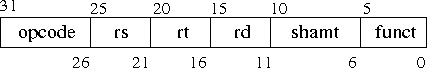
- The opcode is bits 26-31, 6 bits
- The rs is bits 21-25, 5 bits
- The rt is bits 16-20, 5 bits
- The rd is bits 11-15, 5 bits
- shamt is bits 6-10, 5 bits
- funct is bits 0 - 5, 6 bits.
- Uses of these fields
- opcode, funct are opcode bits.
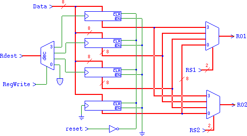
- Look at figure 4.19 page 266
- Trace the path for instruction[31-26]
- Trace the path for instruction[5-0]
- Look at the green sheet for add
- OPCODE/FUNCT 0/20
- As opposed to and 0/21
- rs, rt are source registers for this instruction
- Back to figure 4.15
- These are the values for RS1 and RS2
- So they select what is produced on RO1 and RO2
- rd is the destination register
- Again of figure 4.15 it is the address for the destination or results of the computation.
- We will postpone shamt for the moment.
- We have sufficient information to build the register file.
- There are 32 registers, 0 through 31. (Green sheet, lower left)
- Register 0 is special
- Writes to register 0 do not occur
- It contains 0
- All others can be written to
- Some have special purposes
- But more on that later.
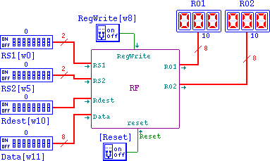
- I will build a 4 register register file
- Because 32 registers just take too much space
- And you get the same idea.
- RS1 and RS2 use a mux to select from the registers for the value of r RO1 and RO2
- Rdest provides the address for a decoder to light the clock for a selected register
- RegWrite enables the decoder
- But we could do this with an and as well
- Output 0 of the decoder is discarded
- I hooked it up to an led to keep tkgate from crashing
- The outputs of the decoder go to the clocks of the registers
- Except register 0, which the clock is hard wired to ground
- Data is just the input to the registers.
- I added a reset input to reset the entire register file.
- This is wired to not(clear) through an inverter.
-
-
- the tkgate file