$\require{cancel}$
AND and OR
- For us, the next two most basic operations are
and and or
- and
-
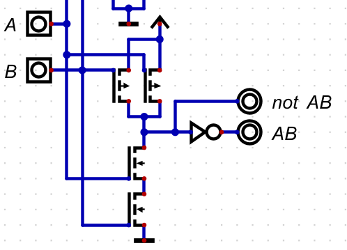
- Please note, my transistor circuit is not optimized.
- nand
- not and.
- f(a,b) = ab
-
- It is my understanding that
- Nand requires fewer transistors than and
- It is one of the tools electrical engineers, computer engineers, ... work with.
- or, nor
-
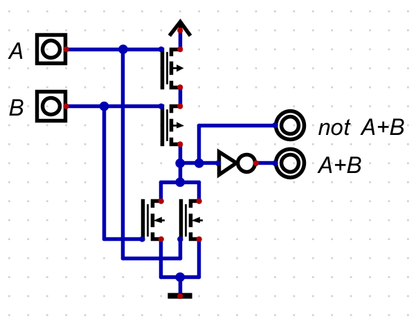
- Again, nor potentially requires fewer transistors.
- So they are commonly used.
- The Digital file for these two.
- Interestingly
nand and nor are universal
- This means that all other logic gates can be built from them.
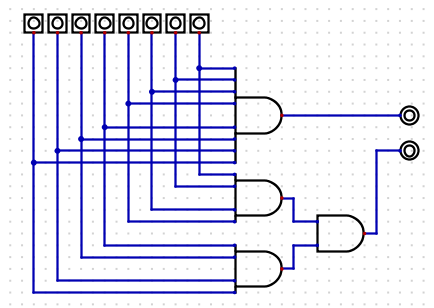
- More than two input gates exist.
- In general they extend the function.
- A three input and gate requres all three inputs to be true for the output to be true.
- A three input or gate requres one or more input to be true for the output to be true.
- A three input xor gate requires exactly one input to be true for the output to be true.
- At the end of chapter 3, Carpinelli discusses practical limitations on gates
- We can design equations, and even digital circuits that we really can't implement.
- Fan-in
- For a gate, this is the maximum number of inputs it can support.
- The more inputs the slower the gate.
- Because there are more transistors requred to accomplish thetask.
- And they can not all operate in parallel.
- Depending on the technology the practial limit is between 2 and 8 inputs.
- Soon we will work on solutions.
- But an 8 input and gate can be accomplished with 2-4 input and 1 normaland gates.
-
- the digital file
- Fan-out
- This is related to the number of other gates that can be connected to the output of a single gate.
- The gate will not produce enough current to drive the connected gates when the number is too high.
- Again depending on technology this can be as low as 4 or as high as 50.
- Again, soon we will do some fixes.
- Propogation Delay
- Each transistor takes some time to switch.
- Generally we idealize ths to be
- Not has a propogation cost of less than 1
- And and Or have a cost of 1 (this should probably be nand and nor)
- Others have a cost of 1 or more.
- We can demo this in Digital
- The Data Graph (under I/O) is helful here.
- Make sure to label all input and output.
- And enable Show single gate steps in the graph
-
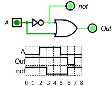
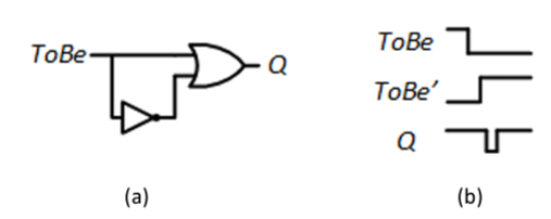
- This circuit should always produce a 1.
- At time 0, A is low, and the output of the circuit is high.
- Sometimes the circut shows out as low for a time step
- At time 2 the circuit has stabalized in the simulation, so the user switches a from Low to High.
- At time 3 (note the delay) not goes low.
- At time 5 the circuit has again stabalized in the simulation, so the user switches A from High to Low
- Note the the not raises to high at step 6
- At the same time, the not was producing a low and A was low so the or gate produces a low for a "time step"
- At time 8 the circuit has stabalized.
- This would not look like this "in the real world"
- The steps would not all be the same size.
- And they would be curves, not steps.
-