$\require{cancel}$
Memory Foundations
- I am using Kann Chapter 9 (sort of)
- This is the start of sequential logic as opposed to combinational logic
- The output of combinational logic circuits depends only on the input.
- Sequential logic circuits have a "memory" or state. So the output is a combination of the state and the input.
- We want to begin to develop registers.
- These seem important as they are the basis for most of the components of our cpu.
- Two types of devices when dealing with memory
- edge triggered: change state when the clock pulse changes from a 0 to a 1.
- level triggerd: change state any time the clock pulse is at a 1.
- These are sometimes called latches
- But we may also use latch for another term.
- We will use edge triggered devices for the most part.
- By the way, the "clock" is not a clock.
- It is a device that pulses from low to high at a regular interval.
- Tell bad joke here.
- We will have inputs to our devices labeled clock, which may or may not be the clock.
- The basis for most memory circuits is a flip-flop.
- There are several types of these.
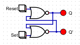
- The easiest is a rs flip-flop
- The rs flip-flop
-

- Two outputs q and q'
- q represents the state of the circuit.
- If it is a 1, the circuit is storing a 1
- If it is a 0, the circuit is storing a 0
- Two inputs, set and reset
- If set is pressed, the circuit will store a 1
- If reset is pressed, the circuit will store a 0
- This is technically a latch, as we don't care about clock.
- You can find videos on line that "reason" this out, but just take it as written.
- Oh and you can get these on a chip.
- This is not the most convenient to use.
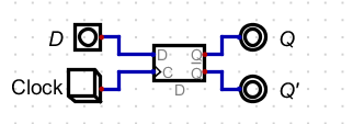
- We will focus on the D flip-flop
-

- Two outputs as above
- Two inputs
- D the data to store
- clock, store the data when this goes
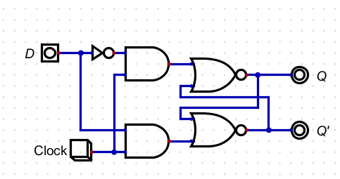
- The picture below is actually a latch
- D flipflops require just a few more gates.
- But you get the idea.
-

- All of these can be purchased in IC form.
- Flipflops have multiple performance times
- The setup time is the amount of time the data should be present on the wires before the clock pulse hits.
- The hold time is how long the data must be stable AFTER the clock pulse
- Read time or access time is the time it takes the circuit to stabilize after the clock pulse.
- Propagation delay
- or clock-to-output time.
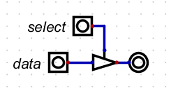
- The tri-state device or driver
-

- Sometimes called three state logic.
- This has two inputs
- in - the data
- select - select
- If select is off, no data passes through the device
- If select is on, data is passed through the device.
- These can be implemented using transistors.
- These devices are very useful when controlling access to a bus.
- only allow one device to write to the bus.
- The digital file
